Anti-Static Injection Molded Box + ESD Foam Inserts + Vacuum-Sealed Shielding Bag
Comprehensive shipping protection for optical modules, MEMS sensors, RF modules and other high-value electronic components
Component Shipping — Every Step Is a Risk
Precision electronic components such as semiconductors, optoelectronics, and sensors face five critical threats during shipping. Without professional packaging, any uncontrolled factor can lead to product failure and significant financial losses.
|
Shipping Threat |
Risk Description |
|
ESD (Electrostatic Discharge) Damage |
Internal circuit breakdown in chips, soaring failure rates, high complaint costs. Latent ESD damage is harder to trace and may only surface during end-user operation |
|
Moisture Ingress |
Moisture-sensitive devices absorb humidity; during reflow soldering, internal moisture expands rapidly causing package cracking (“popcorn effect”), resulting in batch rejection |
|
Vibration & Mechanical Shock |
Fine-pitch lead deformation (pitch as low as 0.4mm), BGA solder ball detachment, optical surface scratching — irreversible yield loss |
|
Electromagnetic Interference (EMI) |
External electromagnetic fields induce voltage differentials during transit, causing performance drift in sensitive devices |
|
Environmental Contamination |
Dust, salt spray, and chemical gases cause solder pad oxidation, reduced solderability, and optical surface contamination |
Three-Layer Protection — Defense in Depth
We provide a complete three-component packaging solution. Each layer addresses an independent protection requirement, combining to form comprehensive shipping protection.
|
Layer |
Component |
Core Function |
Technical Features |
|
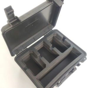
Layer 1 |
Anti-Static Injection Molded Box (ESD Box) |
Rigid physical protection + ESD shielding |
Black conductive plastic, injection molded with integrated hinged lid, prevents collision and compression, provides ESD dissipation |
|
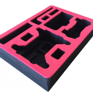
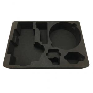
Layer 2 |
ESD Foam Inserts |
Cushioning + Precision positioning |
Custom-cut to product profile, top and bottom foam pads clamp the product for precise positioning, shock absorption, and near-field ESD protection |
|
Layer 3 |
Vacuum-Sealed Shielding Bag (MBB) |
Moisture barrier + EMI shielding |
Metallic shielding bag wraps the entire assembly, vacuum-sealed with desiccant and Humidity Indicator Card (HIC), blocks moisture, EMI, and all external contamination |
Standardized Packaging Process — Step by Step
Following IPC/JEDEC J-STD-033 standards, eight steps transform bare products into shipment-ready condition.
1. Prepare Product — Final-inspected finished components
2. Place Bottom ESD Foam — Custom-cut foam insert placed in the box base
3. Position Product — Product nested into foam cavity for precise alignment
4. Cover with Top ESD Foam — Applies pre-load pressure ensuring zero displacement during transit
5. Close Hinged Lid — Snap-lock closure forms a sealed rigid shell
6. Insert into Shielding Bag (MBB) — Include desiccant and Humidity Indicator Card (HIC)
7. Vacuum Seal — Extract residual air and moisture, heat-seal closure
8. Ship — Product remains in a fully controlled clean micro-environment
7 Standard Sizes — Full Product Line Coverage
No custom tooling required. From compact SFP optical modules to large CFP modules, standard box sizes are ready to use. Foam inserts are custom-cut to your product profile, delivering a cost-effective combination of standard boxes + custom liners.
|
Model |
External Dimensions (L×W×H mm) |
Volume |
Suitable Products |
|
3111 |
74 × 53 × 29 |
~114 cm³ |
SFP optical modules, small sensor chips |
|
3115 |
79 × 54 × 29 |
~124 cm³ |
SFP+ optical modules, MEMS sensor modules |
|
3114 |
74 × 63 × 48 |
~224 cm³ |
Stacked sensors, 3D packaged devices |
|
3112 |
100 × 85 × 33 |
~281 cm³ |
RF front-end modules, Bluetooth/WiFi modules |
|
3113 |
110 × 80 × 45 |
~396 cm³ |
QSFP optical modules, laser components |
|
3110 |
140 × 95 × 38 |
~505 cm³ |
QSFP28/QSFP-DD optical modules, small PCBs |
|
3116 |
190 × 120 × 60 |
~1368 cm³ |
CFP optical modules, large sensor modules, multi-piece kits |
Every Layer — Precisely Targeted
The three-layer system is not over-engineering — each layer targets specific shipping risks, and none can be omitted.
|
Shipping Pain Point |
Consequence Without Professional Packaging |
How Our Solution Addresses It |
|
ESD |
Internal circuits instantly destroyed, batch failures, latent damage hard to trace |
Conductive box + dissipative foam + shielding bag form a complete Faraday cage |
|
Moisture Ingress |
Package cracking during reflow (“popcorn effect”), entire batches scrapped |
Vacuum-sealed MBB removes residual moisture, desiccant + HIC locks humidity below safe threshold |
|
Vibration & Shock |
Fine-pitch lead deformation, BGA ball detachment, optical surface damage |
Rigid box shell resists compression, custom foam precisely positions and absorbs shock energy |
|
EMI |
External fields induce voltage differentials, sensitive device performance drift |
Metallic shielding bag layer provides effective electromagnetic barrier |
|
Contamination |
Solder pad oxidation, optical surface contamination from dust/salt/chemicals |
Vacuum seal creates clean micro-environment, isolating all external contaminants |
One Supplier — Complete Solution
1. One-Stop Procurement — Box + foam + shielding bag from a single supplier. One PO, one contact, one delivery — dramatically simplified sourcing
2. Standard Sizes Ready to Ship — 7 standard specifications cover mainstream electronic component dimensions. No tooling wait, stock available, rapid production line response
3. Custom Foam Cutting — Foam cavities custom-cut to your product’s 3D profile for precise nesting, accommodating any irregular component
4. Production-Line Friendly Design — Hinged lid enables one-hand operation, high-frequency open/close without losing lids, improving packaging efficiency
5. Standards Compliant — Complete solution meets IPC/JEDEC J-STD-033 moisture-sensitive component handling standards, satisfying end-customer audit requirements
6. Cost-Effective Solution — Standard boxes + custom foam eliminates expensive mold costs and lengthy development cycles compared to fully custom injection-molded trays
Custom Packaging Solution for Your Products
Share your product dimensions and protection requirements, and we’ll recommend the optimal box size with a complete quotation for matching foam inserts and shielding bags.
https://www.yufapolymer.com/esd-foam-packaging-for-electronics_c13